Sunday, July 27, 2014

Biasing of a diode

Basically a diode can be biased in two ways-forward biased and reverse biased mode.

  • FORWARD BIASED p-n JUNCTION DIODE:-
 The above image shows the connection type for forward biased diode.Remember that in forward biasing the positive terminal of the battery is connected to p-type and negetive terminal of the battery to n-type.The holes in the p-side are repelled by the positive terminal of the battery while the electrons in the n-side are repelled by the negetive terminal of the battery causing some electrons and holes to enter the depletion region(To know more about depletion region go to-http://dutta60.blogspot.in/2014/07/p-n-junction-diode.html ).Thus the width of the potential barrier as well as the width of the depletion region is reduced as a result of which large number of majority charge carriers can diffuse through the junction.Holes travelling to the right and electrons travelling to the left constitute current in the same direction .So we can say that the resultant current is the sum of currents produced due to holes and electrons.After this an interesting thing happens that is after crossing the junction the holes become minority carriers in the n-region resulting in an injected minority current,and the same is valid for electrons also.Diffusion current can be of substantial amount as the amount of  carriers is large,on the other hand the generation of  carriers also depends upon the degree of biasing.Now for each electron and hole recombination,an electron from the negetive terminal of the battery enters the n-region and after that it drifts towards the juncion.Also in the p-region an electron breaks bond in the crystal as a result of which a hole is created and this hole drifts towards the junction but the electron enters the positive terminal of the battery.So we can conclude that current in the external circuit is due to the movement of electrons,current in p-region is due to holes,and current in n-region is due to electrons.


  • REVERSE BIASED p-n JUNCTION DIODE:-
  The connection here is exactly opposite of what the connection is done for forward-biased mode.The negetive terminal of the battery is connected to the p-side and the positive terminal to the n-side.The holes of the p-side are attracted towards negetive terminal while the electrons in the n-side are attracted towards the positive terminal.As a consequence of which the depletion width is increased due to the increase in uncompensated ions.Now it becomes more difficult for majority carriers to cross over as the resistance offered by the depletion region is enormous .But the movement of the minority carriers is helped by the potential barrier.The rate of generation of minority carriers at a particular temperature is constant as a result of which the current remains the same whether or not voltage is increased or decreased .This current is called the reverse saturation current which is very small.

If you have any questions feel free to ask!! 

Thursday, July 17, 2014

p-n junction diode

Previously,I have mentioned that a diode is a fusion of p and n-type semiconductors,p and n-type materials taken separately has no practical value but when they are combined they give rise to new devices such as transistors,diodes etc.A diode is a device which allows the current to flow in one direction but disallows the reverse.To understand the working you must have the basic knowledge of semiconductors,so here's the link which will help you to do that  http://dutta60.blogspot.in/2014/07/a-complete-guide-to-diodes.html .
The first image is the symbol for p-n junction diode while the other two is how it looks like in real life.
What happens when p and n type semiconductors are clubbed together?
                                     
Sorry for the bad drawing,so as I was saying,the p-region(left portion of the image) has holes which are mobile and negetively charged impurity ions which are immobile whereas the n-region(right side) has positively charged impurity ions which are immobile and free electrons which are mobile.

MOTION OF MAJORITY CHARGE CARRIERS- When the p-n junction is formed diffusion of holes begin from p-region to the n-region and similarly the diffusion of electrons happens on the reverse direction on account of difference in concentration.The movement of both  the holes and electron produces a diffusion current directed from left to right.

Formation of depletion region- one thing that happens during the formation of diffusion current is that recombination takes place near the junction(marked by yellow in the above image) thereby eliminating a hole and an electron in the process.Thereby,leaving uncompensated positive donor ions in the n-region and negetive acceptor ions in the p-region forming the so-called DEPLETION REGION.After this is formed no more diffusion can take place as holes and electrons are both repelled respectively unless some biasing is done (it will be taken up in my next post).The depletion region is also known as space charge region.


Tuesday, July 1, 2014

A complete guide to Diodes

The most widely used circuit element is diode without which many electronic gadgets wouldn't even exist.Now before I begin my lecture on Diode,you must have some preliminary knowledge about semiconductors because a diode is a fusion of semiconductor materials(namely p and n type semiconductors).So,let's start by defining what is a semiconductor?The most common definition you will find is that semiconductor is a material whose conductivity lies between that of a conductor and a insulator.Now, to fully understand the characteristics of a semiconductor it will take a hell lot of time but I will give brief insight so that you have no difficulty in understanding Diode.
SEMICONDUCTOR-
The above diagram is known as the energy band diagram of a semiconductor.Now as you can see from the above image the two energy bands are distinctly separate as there is no overlapping.The empty space between the conduction band and that of valence band is known as forbidden band gap which is roughly 1 eV for a semiconductor.The forbidden gap is an important characteristic or you can say a tool that can predict that a given material is semiconductor,conductor or a insulator.
At absolte zero of temperature,no electrons have the energy to cross the forbidden gap and reach the conduction band but however at room temperature these electrons get enough thermal energy that is greater than the band gap energy to cross the gap and to reach their destination.Thus you can see that this material behaves as a insulator at absolute zero but as a conductor at room temperature.This specific property enables the crystal to differentiate it as the semiconductor.Higher the temperature higher are the chances of electrons to jump to conduction band and so greater is the conductivity.There is also one thing you should know that when electrons leave their postions in the valence band,it leaves some energy level as unfilled.So,these unfilled levels are termed as holes.This are a sort of positive charge carriers and any movement of these carriers will be termed as positive charge moving from one place to another.
Now there are two types of semiconductors -one is intrinsic and the other one is extrinsic.
Intrinsic semiconductor is the pure form of semiconductor and the above explanation is enough to understand intrinsic semiconductor.The real fun begins in extrinsic semiconductor which you must and should learn so as to master Diode completely.
EXTRINSIC SEMICONDUCTOR-This the impure form of semiconductor where doping is introduced.Now let me define Doping for you-"Doping is the process by which impurity in the form of semiconductor atoms is introduced to influence the electrical characteristics of the material".Due to different types of doping two types of  extrinsic semiconductor are available that is p-type and n-type material.

n-type material- 
When a semiconductor such as Silicon and Germanium is doped with pentavalent impurity (Phosphorus,Antimony,Arsenic) we get n-type material.The above diagram is the crystal structure of n-type material .As seen from the figure four out of five electrons occupy covalent bonds.The fifth electron as you can see is loosely bound.The energy required to detach this electron is almost negligible and this energy is easily provided by the thermal agitation of crystal.So, these fifth electron can move freely .When these fifth electron is transferred to the conduction band ,the parent impurity atom becomes positively charged immobile ion.So, in these way each impurity atom donates a free electron to the semiconductor thereby influencing electrical characteristics.This type of semiconductor is also called donor type semiconductor.Here you will also observe that the no. of electrons increase where the holes are in a state of decline.So in an n-type material,electrons are the majority charge carriers and holes fall in the minority group.

p-type semiconductor- 
When silicon and germanium is doped with trivalent impurity(Gallium,Boron),we get p-type semiconductor.The above image shows the crystal structure of p-type.The impurity atom allows electrons to fill only three covalent bonds .The vacancy that exists in the fourth bond constitutes a hole.So,this hole is deliberately created with the purpose that it would accept electrons from the neighbourhood.And when it does a hole is created at that position and this is bright shining example of hole moving from one place to another (+ve charge) as i have mentioned this in my post previously.This is also called acceptor which is justified by the above facts.In a p-type semiconductor holes are the majority and electrons are the minority charge carriers .
The above two facts about majority and minority in both the type of semiconductors forms the basis of understanding Diodes.The full explanation of working of diodes will be mentioned in my next post.Until then Happy Reading.Do bring to my notice if something is wrong!!!!


Saturday, June 21, 2014

LC Filter and pi filter


  •  LC FILTER
                                                           
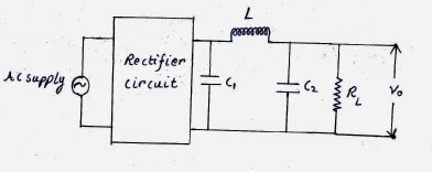
There is not much of an explanation left if you have understood how a inductor and capacitor filter works (working of both filters are given in my previous posts).Let's recapitulate,in an inductor filter the ripple factor is directly proportional to the load resistance but in capacitor filter it is inversely proportional to the load resistance.So the question is what happens if both are present in the same circuit.The answer is that in such a circuit ripple factor becomes almost independent of load resistance.The formula of ripple factor is given by the following expression...............................
                                                           
From the formula it is clear that the ripple factor doesn't depends upon load resistance.
  • Pi-Filter
As you can see from the figure only an additional capacitor is added to the LC filter making it an pi-filter.This type of filter is used when a high DC voltage at low load current is required .As usual the pulsating voltage from the rectifier circuit is fed into the pi-filter circuit.The capacitor (C1) provides low reactance to the ac components as well as high reactance to dc components.The dc components are passed through the inductor as it provides low reactance to the dc components but high reactance to ac components.The capacitor (C2) operates in a similar way as that of  capacitor C1. As a result of this only dc component is available at the output.The formula for ripple factor is given by the following expression ............
There is one disadvantage in pi-filter which is that ripple factor depends upon load resistance whereas in LC filter it is independent.That's it!!!

Thursday, June 19, 2014

Capacitor filter

(picture taken from wikipedia)
The above diagram is the Capacitor filter which generally comprises of a Diode rectifier circuit and a filter circuit where the capacitor is connected in parallel to the load resistance.When a pulasating DC voltage is applied across the capacitor,the capacitor filter removes voltage ripples upto a certain extent but if in addition to it a rectifier circuit is added the output voltage is much better(i.e you can say ripples are removed to a large extent).In order to understand how a capacitor filter works ,you need to have the clear picture of output waveforms in mind .

  • Now what happens is that,in the positive half cycle of output voltage,the capacitor gets charged very quickly to the maximum value.The charging is almost instantaneous as there is no resistance.That is why the capacitor follows the charging voltage.When ac voltage starts to decrease from its maximum value ,the capacitor returns its charge.
  • During the negetive half cycle,output voltage of the rectifier is zero which you can observe from (a) .So what happens is that the capacitor discharges through the load resistance at that time.The discharging time constant is RLC(i.e. the product of load resistance and capacitance).With the increase in the time constant discharge voltage of the capacitor will be less.In reality, you will be astonished to know that discharging time constant is about 100 times larger than that of charging time.This is the reason why a capacitor can maintain a perfect constant voltage across the load resistance.
  • Due to the charging and discharging of the capacitor ,ripples evolve in the output voltage which is much less but still can't be ruled out.The ripple factor is expressed by gamma and is given by the following expression ..........................
                                     
where f is the frequency ,RL is load resistance and C is the capacitance.
In my next post I would explain the working of LC filter(inductor capacitor filter) and pi filter.Stay tuned.If you have any problem just let me know. Happy reading!!
                               

Sunday, June 15, 2014

Filters

To start with let me give you a preliminary idea about a filter.A filter can be natural one,biological one,and also of a psychological one.Here ,I will mention about a technical filter which basically filters out to be FILTER in the subject electronics.So,in many electronic circuits we require direct current(DC) and to convert AC to DC we require a filter which is practically of many types such as inductor filter,capacitor,pi-filter,capacitor-inductor filter and many more.I have mentioned only those filters that i am going to explain on my posts respectively.  Let me excite you by a promise-'you will become expert on this topic provided you have some pre-knowledge about the subject and concentration lapses are/should be negligible'.SO GEAR UP.........
Let me give you a image describing the waveform.
Thye first one is  is taken from the output of an rectifier circuit (e.g.Diode rectifier) and this output voltage is passed on to the filter circuit and the output is similar to the 2nd mage above.Now ,let us start this interesting topic by understanding the inductor filter.
  • INDUCTOR FILTER
From the above figure you can observe that the inductor(L)is placed between the rectifier circuit and the load resistance(RL).Now as i have told you that the rectifier output voltage consists of ac as well as dc components as it is a sinusoidally varying curve.When ac signal is passed through the inductor it provides high impedence to it thereby blocking the signal completely(hint-emf is induced due to constantly changing magnetic flux) but when a dc signal is passed through it,the inductor provides very low impedence and thereby allowing the signal to pass through.So,the ac component is removed but the dc component is allowed to pass.Now,concentrate on the first image where due to the ac components ripple exists.Ripples are considerably decreased but you can't weed it out completely.100% removal is available only in ideal cases(but ideal cases don't occur in reality).
Just look at the image above where i have given a formula for ripple factor denoted by gamma.
RL-This is the load resistance(ohms).
L=This is the inductance in Henry.
w(omega)=Frequency is in Rad/s.
You can observe from the above equation that the ripple factor increases with increasing load resistance but decreases with increasing inductance.
  • PROBLEM TO ENGAGE YOUR NEURONS:-
The output voltage of a full wave rectifier circuit is fed into an inductor filter.Design inductor filter if the ripple factor of filter output voltage is 4% for a load resistance of 100 ohm and the supply frequency is 50Hz.(Ans-L=1.53H)
Stay tuned for more if you have any problems just hit me up.


Friday, June 13, 2014

SMPS (switching mode power supply)

First of all to start with let me give you the full form.S.M.P.S means switching mode power supply.It is also known as PSU(power supply unit),if you have a computer just look at the backside of the CPU you will be able see a huge fan which  basically helps the PSU'S from overheating.The amount of power delivered by this SMPS  depends upon your hardware specs,suppose you basically have a good amount of ram, processor, and a good GPU you will need to have a good quality SMPS which is of say 550V,this is the standard benchmark .In my case what happened is that I bought a Gpu (ATI Radeon HD 6570) which demands higher power and at that moment I had a 450volt SMPS.After injecting my newly aquired hardware I got excited and started playing hardcore games(my first on the list was crysis 3),but my excitation was soon put to end by my Smps which was unable to deliver power and due to which  there was unexpected shutdown everytime I played the game for 5mins.So I had to change my SMPS.


        I bought this SMPS, which is super cool and works with absolutely zero noise.You can buy it too and be safe for the future.          
In extreme cases overheating may cause fire so don't risk it if you experience the same problem. Anyway in this post my objective is to make you understand how a S.M.P.S works,so lets get started.......
In SMPS the input is A.C mains ant the output is D.C.The isolation between the input and output is required.The working of a SMPS can be perfectly understood by the block diagram.
As you can see from the above block diagram the ac mains are first rectified and the rectifier output is smoothed by using a filter and after that smoothed dc is switched at high frequency(typically about 50khz).Smps uses a high frequency MOSFET as a switching transistor with varying duty cycle of the chopper to maintain the output voltage.The switched current flows in the primary circuit of the transformer(for more information please refer to my post about basic idea of a transformer) .After this secondary current from the transformer is rectified and smoothed.And as I have mentioned earlier the control of the output voltage is obtained by the adjustment of  the chopper duty cycle.The main objective of the smps is to convert electrical power efficiently and to transfer power from a source to a load.Smpses can also be used to step down a supply voltage which a transformer alone can do though smpses comprises transformer as  you can see from the above figure.
The above procedures is followed by a basic SMPS.However there are several  types of SMPS which are:
  • Buck or forward converter
  • Bbuck-boost converter
  • Boost or flyback converter
  • Pushpull converter
  • Cuk converter
  • Resonant converter
  • Half-bridge and Full-bridge converters
The choice of SMPS is basically driven by our power needs.Here only the basic idea of SMPS is given.Working of the types of SMPS is more complex but if you know how it works you will be able to understand all those damn converters.Happy Reading!!!